Huawei Server Efforts: Hi1620 and Arm’s Big Server Core, Ares

For four decades today, Arm has been pushing its own attempts to be a large part of their modern day host, the modern day information centre, and at the cloud because a genuine business participant. Arm cores are observed in lots of areas in the server world, with large deployments because of its own smartphone concentrated Cortex core family in large chips. But for those exact same four decades, we’ve been asking a high speed core, to compete in only threaded workloads with x86. That heart is Ares, due out in 2019, and while Arm has not formally lifted the lid to the facts however, Huawei has announced it’s hardware using Ares cores during its centre.
Normally at AnandTech once we talk Huawei, it’s in the context of devices and smartphones like the Mate 20, or smartphone processors such as the Kirin household. Among Huawei’s additional groups is its own Enterprise wing, which is nearly as large, and it produces a great deal of custom silicon and hardware with its in-house design group, HiSilicon. HiSilicon’s remit goes all of the way from smartphones to modems into SSD controls to PCIe controls along with high-performance enterprise compute chips.
. .
Section of this TaiShan household, the Hi1620 would accompany hardware like the Hi1616 in being constructed using Arm IP. The newest Hi1620 was declared as the world’s earliest 7nm chip for the data centre, together with the Ares cores being that which will induce high-performance because of its deployments.
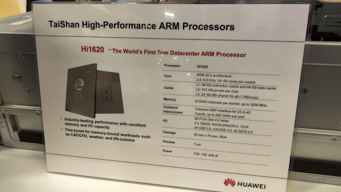
While Huawei did not have some Hi1620 in the series, it had been encouraging the fact it will be a basis in its own portfolio, and lifted the lid on many of important areas of the chip.
The brand new Hi1620 will comprise 24-64 cores per socket, operating from 2.4-3.0 GHz. Every one of those cores are going to have 64KB L1-Data cache and a 64 KB L1-Instruction cache, together with 512KB of personal L2 cache per core. L3 would operate in 1MB/core of cache, up to 64MB. On a scale of a customer Skylake heart, which suggests more L2 cache per core, however less L3. Among the major question marks is to functionality: many sellers are hoping to get an Arm heart with Skylake-levels of raw functionality.
Memory is set in 8 stations around DDR4-3200, along with the processor will encourage a multi-socket setup to 4S, together with the coherent SMP interface capable of 240 GB/s for every chip-to-chip communication. The 4S design would be a totally connected layout.
IO for your Hi1620 is put at 40 PCIe 4.0 lanes, which will be less compared to 46 lanes to the Hi1616, but these ones have been rated for PCIe 3.0. The Hi1620 will even have CCIX support, in addition to double 100GbE MACs, a few USB 3.0, and a few SAS connectivity.
The package listed is 60×75 mm BGA, which provides no real indication into the processor inside. But that is a great deal of balls around the trunk, and the bundle is bigger compared to 57.5×57.5 millimeter layout from the previous generation. Huawei says the Hi1620 is going to be available in TDP ranges from 100W to 200W, together with the varying heart count, but processors will be provided that may be fine for memory bound workloads.
There are still lots of unanswered questions, like the interconnect, but we really wish to get to grips with all the microarchitecture of Ares to discover what’s beneath the hood. Numerous journalists in the show were calling that Arm ought to be having an event from the first half of 2019 to lift the lid onto the plan of the center.